MOU signed for US semiconductor subfab R&D facility
The first such facility in the US is intended to close the semiconductor industry's most critical sustainability gap.
International SubFAB Research Labs (ISRL USA) and AI Infrastructure Partners (AIIP) have announced a memorandum of understanding to design, build and operate the US’ first purpose-built R&D facility dedicated to semiconductor subfab infrastructure, which they say provides a critical step towards enabling sustainable, high-volume semiconductor manufacturing at scale.
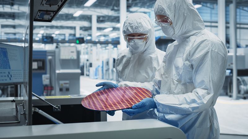
They claim the platform will support independent device manufacturers (IDMs), foundries, OEMs, subfab suppliers, materials companies and research institutions.
AIIP will design, build and own the facility and infrastructure. ISRL USA will lead technical operations, research programmes, and the industry-neutral, multi-member platform.
The facility will provide a shared Infrastructure-as-a-Service (IaaS) environment, allowing semiconductor companies to conduct pre-competitive research, validate technologies and generate compliance-ready data say the partners.