UK-based Paragraf expands graphene electronics manufacturing capability
The company says it has produced the first 6-inch graphene wafer at its new site in Huntingdon.
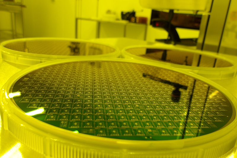
The wafer contains graphene field-effect transistors (GFETs) fabricated using Paragraf’s proprietary process, in which graphene is grown directly on silicon.
Until now, Paragraf has produced GFETs on 2-inch sapphire wafers. While other approaches to GFETs on silicon typically rely on transferring graphene from a growth substrate, often introducing metallic contamination, Paragraf’s direct-on-silicon process reportedly preserves material purity and device integrity in a move to mainstream semiconductor manufacturing.
The transition from 2-inch to 6-inch wafers is said to be a major milestone, enabling higher throughput, improved uniformity and closer alignment with established semiconductor fabrication infrastructure to accelerate the development of scaleable graphene-based electronic and sensing devices.